
We understand that engineers require boards that are reliable and can handle more current and maintain the correct signals. Cheap Hybrid Pcb choices can seem appealing, but the right board spec affects thermal performance and signal integrity. Herein we discuss the reasons why 2 oz finished copper PCBs and stepped-hole routing are important in chargers, medical equipment, and high-speed systems.
Cheap Hybrid PCB options may work when current demands are low, but for power-dense designs a 2 oz finished copper PCB is the safer choice. Cheap Hybrid Pcb selections that rely on 1 oz copper can produce hot spots and higher conductor loss under load. Hybrid PCB buyers should balance cost with required performance to avoid field failures.
Why thick copper matters
Two ounces of copper per square foot is contained on a 2 oz completed copper PCB. The increased weight of copper reduces the level of conductor resistance and enhances thermal control. In comparison to 1 oz boards, 2 oz have higher current density and can withstand continuous loading better. This is essential in the charging of circuits and power adapters.
Manufacturing and process controls
Copper plating is a process that needs to be controlled. Popular processes would consist of determining area and current, plate vias with pulse current, checking coverage by specifically inspecting early, and maintaining uniform spacing of substrates. Proper process control helps in eliminating voids, finish the inside of holes with a metallic finish, and eliminates darkening of the surface of subsequent panels.
High-speed signal considerations
Stepped-hole PCBs and disciplined layer stack-ups refer to high-speed transmission. Reflections, crosstalk and insertion loss have impacts on timing and amplitude as the clock frequencies increase. Dielectric thickness, roughness of the material and line width, spacing and dielectric thickness all affect the signal integrity and insertion loss.
Technical highlights to request
- Layers: up to 8 with laser drilling for microvias.
- Materials: low-loss FR-4 for better SI.
- Dielectric thickness: example 2.0 mm core.
- Finished copper: 2 ounce for heavy-current boards.
- Min track/gap: 0.12 mm / 0.12 mm.
- Surface finish: ENIG or OSP as required.
Choosing the Cheap Hybrid Pcb solution
Engineers often search for Hybrid PCB vendors to reduce BOM cost. A Hybrid Pcb can be acceptable if the application has modest current and thermal needs. But when power density or signal fidelity are critical, a Cheap Hybrid Pcb using thinner copper or lower-grade material may not meet specs. Defeat your thermal targets and impedance objectives prior to choosing a supplier.
When to use stepped-hole designs
Interfaces Modules and control impedance on the layer to layer transitions are interfaced with stepped holes. They are useful in modules with high speed and multi-board systems. Ensure that the manufacturer observes appropriate lamination, laser drilling, and exposure technology and processes to achieve uniformness.
Cost and lead time considerations
Price and delivery are issues that many teams ask. A Cheap Hybrid Pcb may save immediate cost but can increase rework and warranty expense if underspecified. Check the lead time of thick copper plating and ensure quality checks before manufacturing.
Product description
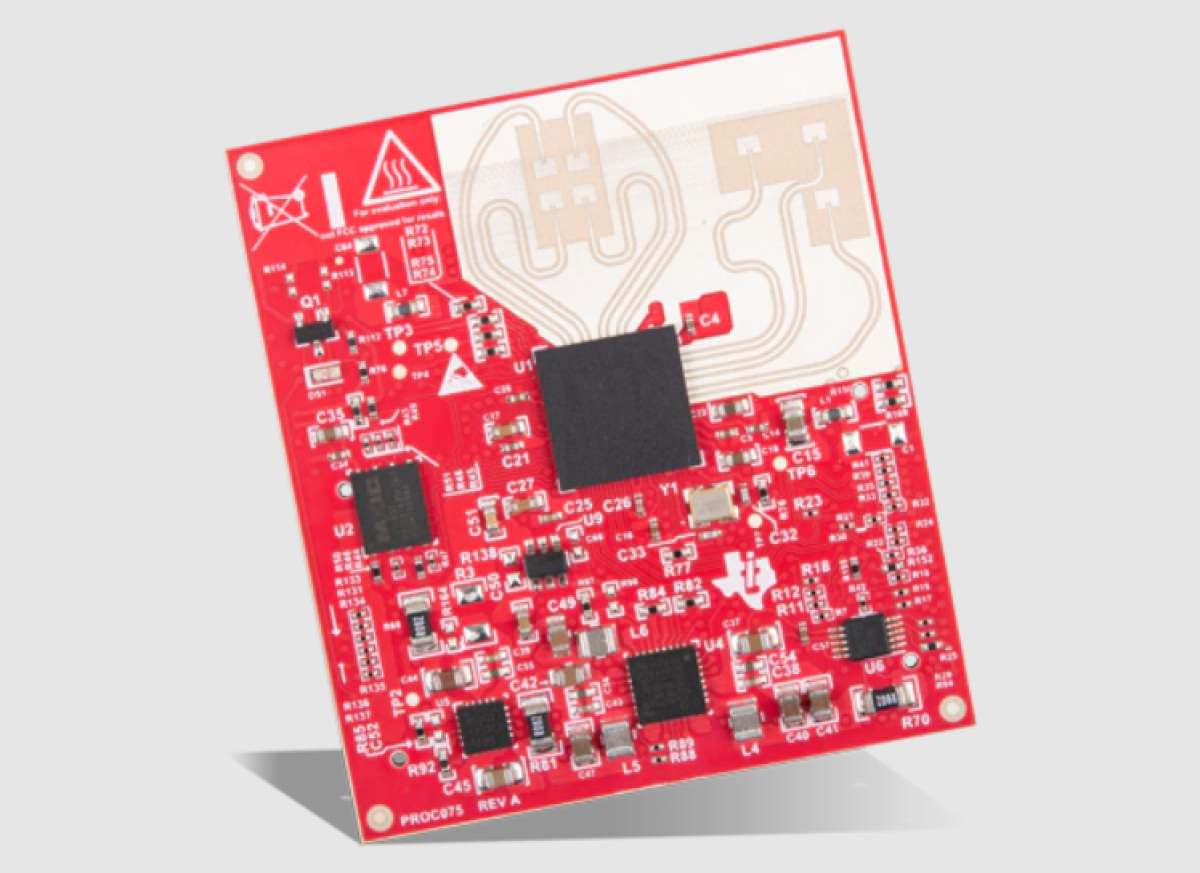
Board recommendation: 8-layer PCB in low loss FR-4 with 2 oz finished copper outer, laser-drilled microvias, 2.0 mm dielectric thickness, minimum 0.12 mm track/gap. This arrangement is appropriate to the medical ozone equipment, chargers and high speed communication modules that need both the ability to handle power and clean signals.
FAQ
Q: What is the relationship between copper weight and reliability?
A: Increased copper weight reduces resistance and heat dispersion, which creates hotspots and enhances long term reliability.
Q: Is it possible to use thick copper in the flexible circuits?
A: Yes, however flexible designs tend to have smaller copper weights; the 2 oz is selective.
Q: Which tests are used to test signal integrity?
A: Check SI on your frequency range by inserting a load on the input, measuring the resulting output, and recording the loss length.
Get Started with BS Interconn
In case you require heavy-current or high-speed board and stack-up, material, and production controls, contact BS Interconn. Send your Gerbers and needs to us, and we will advise you on what will be the most economical way out.
Read Also : Article Nest